- 您现在的位置:买卖IC网 > Sheet目录516 > SIRA10DP-T1-GE3 (Vishay Siliconix)MOSFET N-CH 30V 30A SO-8
�� �
�
�SiRA10DP�
�www.vishay.com�
�N-Channel� 30� V� (D-S)� MOSFET�
�Vishay� Siliconix�
�60�
�PRODUCT� SUMMARY�
�V� DS� (V)� R� DS(on)� (� ?� )� (MAX.)�
�0.0037� at� V� GS� =� 10� V�
�30�
�0.0050� at� V� GS� =� 4.5� V�
�I� D� (A)� a,� g�
�60� g�
�g�
�Q� g� (TYP.)�
�15.4� nC�
�FEATURES�
�?� TrenchFET� ?� Gen� IV� power� MOSFET�
�?� 100� %� R� g� and� UIS� tested�
�?� Material� categorization:� ?�
�For� definitions� of� compliance� please� see�
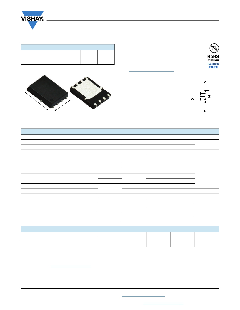
�PowerPAK� ?� S� O-8� S� in� g� le�
�D�
�www.vishay.com/doc?99912�
�D�
�5�
�D�
�6�
�D�
�7�
�8�
�APPLICATIONS�
�?� High� power� density� DC/DC�
�D�
�?� Synchronous� rectification�
�?� VRMs� and� embedded� DC/DC�
�5m�
�6.�
�15�
�m�
�m�
�1�
�5.1�
�m�
�4�
�G�
�3�
�S�
�2�
�S�
�1�
�S�
�G�
�Top� View�
�Ordering� Information� :� ?�
�Bottom� View�
�S�
�N-Channel� MOSFET�
�SiRA10DP-T1-GE3� (Lead� (Pb)-free� and� Halogen-free)�
�ABSOLUTE� MAXIMUM� RATINGS� (T� A� =� 25� °C,� unless� otherwise� noted)�
�PARAMETER�
�Drain-Source� Voltage�
�Gate-Source� Voltage�
�T� C� =� 25� °C�
�SYMBOL�
�V� DS�
�V� GS�
�LIMIT�
�30�
�+20,� -16�
�60� g�
�UNIT�
�V�
�Continuous� Drain� Current� (T� J� =� 150� °C)�
�T� C� =� 70� °C�
�T� A� =� 25� °C�
�I� D�
�60� g�
�25� b,� c�
�Pulsed� Drain� Current� (t� =� 100� μs)�
�Continuous� Source-Drain� Diode� Current�
�Single� Pulse� Avalanche� Current�
�Single� Pulse� Avalanche� Energy�
�T� A� =� 70� °C�
�T� C� =� 25� °C�
�T� A� =� 25� °C�
�L� =� 0.1� mH�
�I� DM�
�I� S�
�I� AS�
�E� AS�
�23� b,� c�
�140�
�34� g�
�4.2� b,� c�
�20�
�20�
�A�
�mJ�
�T� C� =� 25� °C�
�40�
�Maximum� Power� Dissipation�
�T� C� =� 70� °C�
�T� A� =� 25� °C�
�P� D�
�26�
�5� b,� c�
�W�
�T� A� =� 70� °C�
�3.2� b,� c�
�Operating� Junction� and� Storage� Temperature� Range�
�Soldering� Recommendations� (Peak� Temperature)� d,� e�
�T� J� ,� T� stg�
�-55� to� 150�
�260�
�°C�
�THERMAL� RESISTANCE� RATINGS�
�PARAMETER�
�SYMBOL�
�TYPICAL�
�MAXIMUM�
�UNIT�
�Maximum� Junction-to-Ambient� b,� f�
�Maximum� Junction-to-Case� (Drain)�
�t� ?� 10� s�
�Steady� State�
�R� thJA�
�R� thJC�
�21�
�2.5�
�25�
�3.1�
�°C/W�
�Notes�
�a.� Based� on� T� C� =� 25� °C.�
�b.� Surface� mounted� on� 1"� x� 1"� FR4� board.�
�c.� t� =� 10� s.�
�d.� See� solder� profile� (� www.vishay.com/doc?73257� ).� The� PowerPAK� SO-8� is� a� leadless� package.� The� end� of� the� lead� terminal� is� exposed� copper�
�(not� plated)� as� a� result� of� the� singulation� process� in� manufacturing.� A� solder� fillet� at� the� exposed� copper� tip� cannot� be� guaranteed� and� is� not�
�required� to� ensure� adequate� bottom� side� solder� interconnection.�
�e.� Rework� conditions:� Manual� soldering� with� a� soldering� iron� is� not� recommended� for� leadless� components.�
�f.� Maximum� under� steady� state� conditions� is� 70� °C/W.�
�g.� Package� limited.�
�S14-0158-Rev.� B,� 03-Feb-14�
�1�
�Document� Number:� 63820�
�For� technical� questions,� contact:� pmostechsupport@vishay.com�
�THIS� DOCUMENT� IS� SUBJECT� TO� CHANGE� WITHOUT� NOTICE.� THE� PRODUCTS� DESCRIBED� HEREIN� AND� THIS� DOCUMENT�
�ARE� SUBJECT� TO� SPECIFIC� DISCLAIMERS,� SET� FORTH� AT� www.vishay.com/doc?91000�
�发布紧急采购,3分钟左右您将得到回复。
相关PDF资料
SIS412DN-T1-GE3
MOSFET N-CH D-S 30V 1212-8 PPAK
SIS426DN-T1-GE3
MOSFET N-CH 20V 35A 1212-8
SIS436DN-T1-GE3
MOSFET N-CH D-S 25V PPAK 1212-8
SIS452DN-T1-GE3
MOSFET N-CH D-S 12V 1212-8 PPAK
SIS456DN-T1-GE3
MOSFET N-CH 30V 1212-8 PPAK
SIS468DN-T1-GE3
MOSF N CH 80V 30A 1212-8 PWR PK
SIS892ADN-T1-GE3
MOSFET N-CH 100V D-S PPAK 1212
SIS902DN-T1-GE3
MOSFET N-CH D-S 75V 1212-8 PPAK
相关代理商/技术参数
SIRA12DP
制造商:VISHAY 制造商全称:Vishay Siliconix 功能描述:N-Channel 30 V (D-S) MOSFET
SIRA12DP-T1-GE3
功能描述:MOSFET 30V 4.3mOhm@10V 25A N-Ch G-IV
RoHS:否 制造商:STMicroelectronics 晶体管极性:N-Channel 汲极/源极击穿电压:650 V 闸/源击穿电压:25 V 漏极连续电流:130 A 电阻汲极/源极 RDS(导通):0.014 Ohms 配置:Single 最大工作温度: 安装风格:Through Hole 封装 / 箱体:Max247 封装:Tube
SIRA14DP
制造商:VISHAY 制造商全称:Vishay Siliconix 功能描述:N-Channel 30 V (D-S) MOSFET
SIRA14DP-T1-GE3
功能描述:MOSFET 30V 5.1mOhm@10V 20A N-Ch G-IV
RoHS:否 制造商:STMicroelectronics 晶体管极性:N-Channel 汲极/源极击穿电压:650 V 闸/源击穿电压:25 V 漏极连续电流:130 A 电阻汲极/源极 RDS(导通):0.014 Ohms 配置:Single 最大工作温度: 安装风格:Through Hole 封装 / 箱体:Max247 封装:Tube
SIRA18DP-T1-GE3
功能描述:MOSFET 30V 7.5mOhm@10V 13.3A N-Ch G-IV
RoHS:否 制造商:STMicroelectronics 晶体管极性:N-Channel 汲极/源极击穿电压:650 V 闸/源击穿电压:25 V 漏极连续电流:130 A 电阻汲极/源极 RDS(导通):0.014 Ohms 配置:Single 最大工作温度: 安装风格:Through Hole 封装 / 箱体:Max247 封装:Tube
SIRD107-1
制造商:Panasonic Industrial Company 功能描述:BASE
SIRD21-1
制造商:Panasonic Industrial Company 功能描述:TRAVERSE BASE
SIRD42-5
制造商:Panasonic Industrial Company 功能描述:SUB ONLY CLAMP